

Roughly 65% of prototype asset trackers fail early field testing because passive component parasitic capacitance pulls the 32.768 kHz RTC crystal off frequency, preventing the MCU from entering deep sleep. Executing a successful Custom PCB Design for Tracking Devices requires bridging strict RF layout constraints with microampere-level power gating. Standard dev boards won’t cut it. They waste up to 80% of your power budget through active regulators and poor ground plane design.
This guide gives you the precise engineering parameters required to take a tracker from initial schematic to production-ready hardware. You will work through coplanar waveguide routing, antenna matching networks, low-dropout regulator selection, and power-gating topologies that drop sleep currents below 5 µA.
Doing this right takes serious effort. Expect to spend hours tuning matching components on a vector network analyzer, scrubbing your layer stackup for EMI, and debugging board-level leakage paths. But once your design lands, your hardware will survive real-world deployments intact.
Why Is Custom PCB Design for Tracking Devices Necessary Over Off-the-Shelf Modules?
Off-the-shelf modules waste 70% of board space on unneeded interfaces. Purpose-built hardware enables rigid-flex contours, high-density interconnect (HDI) routing, and component-level power gating, dropping sleep current to microamps.
Engineered Hardware vs. Off-the-Shelf Breakouts
| Metric | Off-the-Shelf Board | Custom Tracking PCB |
|---|---|---|
| Sleep Current | 1.5 mA to 5 mA | 3 µA to 12 µA |
| Board Thickness | 1.6 mm rigid | 0.4 mm rigid-flex |
| Component Density | Low (0603 passive min) | High (0201/01005 HDI) |
Breakouts suit early firmware testing. They fail in rugged enclosures. Unnecessary USB transceivers and linear regulators waste energy. A 2.5 mA idle draw kills a 500 mAh battery in 8 days. Dropping sleep draw to 4 µA extends field life past 3 years.
Fitting a cellular modem, GNSS receiver, nano-SIM slot, and 9-axis MEMS accelerometer into tight housings requires blind vias and 0201 passives. Shifting trace clearances near battery clips by 0.15 mm creates EMI coupling.
Relying on custom PCB design services provides the HDI layer stackups, low-noise RF traces, and power-gating topologies required for field reliability. You avoid costly revs and keep BOM targets intact.
- Eliminate parasitic drain from power LEDs and onboard UART chips.
- Flex thin circuit layers around lithium polymer batteries to maximize space.
How Do You Choose Between GNSS, Cellular, and BLE Architectures for Location Tracking?
Architectural Trade-offs and Decision Criteria
GNSS active acquisition draws 20 mA to 40 mA with a 30 seconds cold start. Cellular triangulation offers 100 meters accuracy at under 15 µA sleep current.
When designing a pet tracking PCB, update schedules under two minutes require rechargeable lithium chemistry for your board.
| Architecture | Active Current | Operational Range | Location Accuracy |
|---|---|---|---|
| Multi-Constellation GNSS | 25 mA – 45 mA | Global Outdoor Direct Line-of-Sight | 1.5 m – 5 m |
| LTE-M / NB-IoT | 100 mA – 250 mA Tx Peak | Global Cellular Network Range | 100 m – 1000 m |
| Bluetooth Low Energy (BLE 5.x) | 4 mA – 8 mA | Local Proximity (Under 100 m) | 1 m – 3 m (RSSI / AoA) |
What Is the Ideal Layer Stackup and Antenna Matching Design for GPS Trackers?
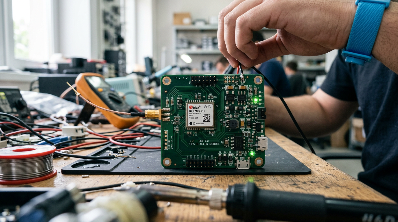
The ideal layer stackup for a GPS tracker uses a 4-layer configuration: Top Signal, Inner Ground, Inner Power, and Bottom Signal. Layer 2 serves as a continuous ground plane directly beneath the 1.575 GHz RF microstrip, maintaining a strict 50-ohm characteristic impedance and securing a VSWR below 1.5 with a Pi-matching network.
Stackup Setup and Noise Isolation
When executing custom PCB design for tracking devices, stackup spacing dictates your RF integrity. Place your RF feedline on Layer 1 over an uninterrupted Layer 2 ground plane. In early builds, digital switching noise from a 2.1 MHz DC-DC buck regulator coupled directly into the Low-Noise Amplifier (LNA) supply trace. That ripple degraded carrier-to-noise density (C/N0) by 12 dB-Hz. Solve this by isolating the LNA power rail using a dedicated ferrite bead with 600-ohm impedance at 100 MHz alongside 10 pF and 100 nF decoupling capacitors placed within 2 mm of the LNA pin.
Antenna Pi-Matching and VNA Calibration
Proper antenna tuning determines the function and design of GPS PCBs. Calibrate your Vector Network Analyzer (VNA) using a standard 1-port SOLT procedure across a 1.50 GHz to 1.65 GHz sweep. In your CAD software—such as KiCad or Altium—calculate a 0.50 mm microstrip width over a 0.20 mm FR4 dielectric layer (εr = 4.5) to achieve 50-ohm impedance. Tune the Pi-matching network using a 5.6 nH series inductor paired with 1.2 pF and 0.8 pF shunt capacitors. This specific combination drops S11 reflection down to -16.5 dB, guaranteeing maximum energy transfer at 1.57542 GHz.
Why Do Most Tracking PCB Prototypes Fail in Field Deployment?
Most tracking PCB prototypes fail in the field because lab bench conditions mask physical realities like casing detuning, un-gated power leaks, and thermal trapping inside sealed enclosures. Open-source designs rarely account for the dielectric constant of an IP67 housing, which instantly shifts antenna resonant frequencies and drops carrier signal strength below usable margins.
When executing Custom PCB Design for Tracking Devices, standard layouts break down under real-world stress due to three main causes:
- Antenna detuning from plastic housing: Placing a 1575.42 MHz ceramic GPS patch antenna inside a 3mm polycarbonate enclosure shifts its center frequency down by 15–30 MHz through dielectric loading. Without tuning via a vector network analyzer inside the final casing, lock times multiply and signal attenuation spikes.
- Un-gated sleep leakage: A 10 kΩ pull-up resistor on an I2C sensor bus tied to an un-gated rail drains 330 µA continuously in deep sleep. That tiny leak destroys a multi-year coin cell power budget in six weeks.
- Thermal trapping in IP67 seals: LTE modules draw 2A peak pulses during transmission. In an unventilated IP67 enclosure, rapid uplink cycles drive internal ambient temperatures past 85°C, triggering thermal regulator shutdowns and clock oscillator drift.
Community schematic templates skip high-side load switch isolation and localized copper thermal relief planes. Relying on these reference designs for your first location tracker PCB build works fine on a bench. But long-term reliability demands re-tuning RF paths inside the final enclosure shell and aggressively power gating every peripheral rail.
How Do You Implement Low-Power Firmware States and Power Gating Circuitry?
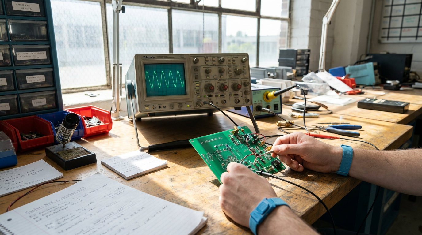
Implementing low-power firmware states and power gating requires isolating peripheral ICs using P-channel MOSFET load switches controlled by MCU GPIOs, cutting quiescent leakage. Pair hardware cutoffs with low-power firmware sleep modes triggered by RTC interrupts or accelerometer motion thresholds, driving active tracking power down from a 45mA active tracking state to a 3.8µA deep sleep state.
Hardware Power Gating Setup
GNSS receiver modules drain batteries rapidly if left powered in standby mode. Connect a high-side P-channel MOSFET between the system power rail and the GNSS VCC pin. Pull the gate high with a 100kΩ resistor to keep the switch off by default. Drive the gate low through an MCU GPIO pin or N-channel driver to energize the module only during satellite acquisition. This setup drops power draw from a 45mA active tracking state to 3.8µA deep sleep, preventing parasitic leakage through RX/TX lines by setting those GPIO pins to analog high-impedance before gating off power.
Firmware Interrupts and Fabrication Rules
Configure your microcontroller to enter deep sleep immediately after publishing coordinates. Set an onboard RTC to fire an external wake-up interrupt every four hours for stationary check-ins. For motion-based tracking, configure an ultra-low-power accelerometer to trigger a hardware interrupt when movement crosses a 35mg threshold for longer than 20ms. When routing dense interconnects for Custom PCB Design for Tracking Devices, refer to a wearable PCB online fabrication guide. Standard automated board houses require strict 4-mil trace/space tolerances, 0.8mm board thickness, and high-density interconnect rules to prevent solder bridging between tiny 0402 components and load-switch packages.
What Is the 3W Rule for PCB Design and How Does It Prevent RF Interference?
The 3W rule states that the center-to-center distance between two adjacent microstrip traces must equal at least three times the trace width. This physical separation lowers capacitive crosstalk and mutual inductive coupling by roughly 70%, protecting sensitive traces in dense board layouts.
In a compact layout for custom PCB design for tracking devices, fast digital edges cause severe RF performance loss. A 24 MHz SPI clock bus driving an onboard IMU creates sharp square waves rich in high-order harmonics. If routed parallel to a 1575.42 MHz GPS receiver feedline without proper spacing, magnetic and capacitive coupling injects broadband noise into the low-noise amplifier, degrading carrier-to-noise ratio (C/N0) by 3 dB to 6 dB.
When to Implement 10W Spacing and Guard Vias
High-power cellular trackers transmitting at +23 dBm demand aggressive signal isolation. A standard 3W gap cannot suppress high-frequency power amplifier harmonics or DC-DC buck converter switching spikes.
- 10W Rule: Separate RF traces from aggressive switching nodes by ten trace widths center-to-center, suppressing electromagnetic coupling by over 98% and reducing crosstalk to under -40 dB.
- Guard Via Fences: Place grounded vias along coplanar waveguides at a pitch under lambda/10 (roughly 1.8 mm for GPS L1) to tie top ground floods to the internal plane when layout gaps fall below 3W.
As documented in almost every practical forum guide for GPS tracking PCBs, spatial separation rules offer zero protection if you split the reference plane. Routing traces over ground cutouts forces return currents to loop, creating efficient loop antennas that completely undermine your 3W isolation.

Can ChatGPT Do PCB Design or Generate Reliable Gerber Files?
ChatGPT cannot generate reliable Gerber files or directly design physical PCB layouts. While AI models excel at writing basic scripting plugins or organizing bill-of-materials data, they cannot perform spatial routing, calculate 50-ohm RF trace impedance, or model parasitic capacitance and thermal dissipation across solid copper planes.
Where Generative AI Fails in EDA Workflows
Generative AI frequently hallucinates IC pinouts and lacks 3D spatial awareness. In custom PCB design for tracking devices, an inaccurate trace width calculation or missing return path will degrade your GNSS receiver sensitivity by 10 dB or corrupt cellular transmission under 4G burst loads. LLMs do not run finite element method (FEM) solvers. They cannot predict how a 4-layer 1.6mm FR-4 stackup affects differential pair skew, nor can they handle thermal plane relief near power-gating MOSFETs drawing peak currents over 2A. Text-based AI cannot output valid Gerber RS-274X coordinate geometry without introducing syntax corruption that fails factory CAM checks.
Safe Automation vs. Human Sign-Off
Treat AI as a helper for low-risk administrative tasks. Let it write Python scripts for KiCad to automate silkscreen alignment, format netlists, or parse datasheet tables. Leave physical schematic capture, stackup rules, and Gerber export to dedicated EDA software verified by human sign-off. For university students exploring viva safe hardware project ideas, using AI to draft board automation scripts while personally routing the antenna matching network demonstrates true engineering discipline without risking non-functional hardware during your final bring-up.
How Do You Route High-Frequency RF Traces and Antenna Feedlines?
Route 1.575 GHz GPS and 2.4 GHz BLE traces using grounded coplanar waveguide (GCPW) geometry to maintain 50-ohm impedance over an unbroken Layer 2 ground plane. Apply 3W copper pour clearance and 45-degree mitered bends. Space feedline ground vias at λ/10 intervals—roughly 6 mm for 2.4 GHz on FR-4.
Altium’s high-speed design guidelines emphasize precise stackup impedance control alongside automated end to end tracking of PCB design constraints. To pass FCC Part 15 or CE RED testing, enclose GNSS front-ends in a soldered metal shielding can secured by ground vias spaced 2 mm to 3 mm apart.
How Much Does It Cost to Have a Custom PCB Design Built and Assembled?
Building a custom tracking device PCB costs between $1,000 and $5,000 for low-volume prototypes, while high-volume production drops unit prices under $15. Initial Non-Recurring Engineering (NRE) design fees account for $500 to $3,000 of that initial budget, while bare board fabrication and assembly stencil setup fees make up the remainder.
Breakdown of Prototyping vs. Volume Costs
When executing custom PCB design for tracking devices, your total expense divides between fixed engineering overhead and variable production charges. Engineering providers offering turnkey electronic design services charge NRE fees to convert your architecture block diagram into finished Gerber, ODB++, or IPC-2581 manufacturing files.
Typical prototype expenses split into three distinct categories:
- Schematic & Layout Engineering: $500 to $3,000 depending on multi-constellation RF complexity.
- Bare Board Fabrication: $20 to $100 for an initial batch of 5 to 10 prototype boards.
- SMT Stencil & Setup: $15 to $50 for laser-cut stainless steel stencils and automated feeder setup.
Optimizing Unit Economics at Scale
Single prototype units cost between $100 and $250 per assembled board due to SMT line configuration overhead. Scaling past 1,000 units brings component reel discounts and automated throughput into play, reducing per-unit assembly costs down to $12–$25.
You keep expenses under control by choosing standard 0402 passive components instead of 0201 packages. Standard 0402 passives lower pick-and-place defect rates. Furthermore, sticking to low-cost 4-layer stackups (such as 1.6mm FR-4 with 1oz copper) avoids custom lamination surcharges. Avoid blind or buried vias unless high-density micro-BGA packages leave you no choice.
How Do I Build My Own GPS Tracker from Schematic to Enclosure?
Building a custom GPS tracker requires selecting an integrated MCU and GNSS module, capturing the schematic in software like KiCad, laying out RF trace paths with 50-ohm impedance control, and fitting the assembled board into an IP67 enclosure after validating power draw and cold-start lock times on the bench.
From Schematic to Hardware Deployment
Executing a custom PCB design for tracking devices requires a disciplined, step-by-step workflow from part selection to physical housing:
- Component Selection: Pair an ESP32-C3 microcontroller with a u-blox MAX-M10S GNSS module, an MCP73831 battery charger circuit, and a 3.7V LiPo cell driven by an ultra-low quiescent LDO like the AP7361C.
- Schematic & PCB Layout: Draft your schematic in KiCad or EasyEDA. Set DRC constraints to 0.15mm clearance and 0.2mm trace width. Route a 50-ohm coplanar waveguide feedline directly to your passive ceramic patch antenna.
- Ground Planes: Flood top and bottom layers with copper ground plane pours, placing a dense array of via fences around the RF trace to isolate RF energy from switching noise.
- Benchtop Validation: Profile power draw using a benchtop multimeter to confirm sleep states under 15µA. Verify outdoor cold-start TTFF (Time-To-First-Fix) hits 26 seconds, dropping to 1 second during warm starts.
- 3D Enclosure Fit Check: Export your populated board as a 3D STEP file into Fusion 360 to verify mechanical clearance for battery connectors, antenna orientation, and mounting bosses before 3D printing.
This end-to-end engineering pipeline offers strong practical value when executing fyp ideas for engineering students who need to deliver reliable, field-ready physical hardware.
Which Online PCB Fabrication Services Offer Fast Prototyping and SMT Assembly?
Fast prototyping and SMT assembly for custom PCB design for tracking devices rely on vendors like JLCPCB, PCBWay, and ALLPCB. JLCPCB excels at fast turnaround on standard FR4 layers, while PCBWay leads in RF substrates like Rogers 4350B, and ALLPCB offers automated turnarounds for high-speed production runs.
| Platform | SMT Turnaround | In-Stock Components | RF Substrate Support |
|---|---|---|---|
| JLCPCB | 24–48 hours | 500,000+ parts | Standard FR4 SMT |
| PCBWay | 3–5 days | Custom global sourcing | Rogers 4350B stackups |
| ALLPCB | 48–72 hours | Essential passives | Special order laminates |
Substrate Selection and Turnkey Scaling
Standard FR4 works well for basic power distribution and slow digital logic. However, 1.575 GHz GNSS receivers and 2.4 GHz Wi-Fi antenna feedlines require predictable dielectric constants. PCBWay easily supports hybrid stackups using Rogers 4350B over FR4 inner cores, keeping RF attenuation below 0.1 dB/cm. JLCPCB limits low-cost automated SMT to standard FR4 laminates, which causes higher RF signal loss on compact tracker layouts. Short traces mitigate this, but tight designs suffer. ALLPCB sits in the middle, offering fast turnaround for standard substrates while charging premium expediting fees for custom RF stacks.
When analyzing a robotics hardware integration case study, rapid turnkey prototyping demands balancing off-the-shelf part libraries against long component lead times. Moving from five prototype boards into full turnkey box-build production shifts your engineering focus. You must verify component sourcing channels, validate panelization tooling, demand X-ray inspection for fine-pitch BGAs, and confirm that enclosure fitments pass vibration testing. Skipping these steps risks costly line re-tooling.
Before you route your first trace in your EDA tool, measure the sleep current draw of your MCU and cellular modem on a breakout board using a dedicated current profiler. You want to see your sleep baseline flatline below 15 µA without floating GPIO pins causing leakage spikes. That stable microamp line is your signal that your power gating schematic actually works before you order physical copper.
A custom board will not fix flawed system architecture or broken power math. If your design demands a 1-second GNSS update rate on a 200 mAh battery, custom routing cannot beat physical power limits. Do not bother building custom hardware if your enclosure fits standard development kits and off-the-shelf modules meet your thermal spec. Custom layouts exist for tight physical constraints, custom antenna matching, and strict millimeter-level spatial constraints. Validate your sleep currents on the bench first, lock down your schematic, and only then start your stackup layout.
Frequently Asked Questions
How much does it cost to have a custom PCB design?
Custom PCB design costs range from a few hundred dollars for simple two-layer boards to over $10,000 for complex multi-layer tracking devices with RF integration. Total pricing depends on schematic complexity, layer count, component availability, and required certifications like FCC or CE. You can optimize costs by selecting standard component footprints and reducing board stack-up layers during early prototyping.
Can ChatGPT do PCB design?
ChatGPT cannot directly generate physical PCB layout files, but it can assist you by writing code scripts, recommending schematics, and drafting design specifications. While it helps brainstorm component selection or write Python scripts for CAD tools like KiCad, you still need dedicated EDA software to route traces and handle signal integrity. You must manually verify all AI-generated pinouts and netlists before fabrication.
What is the 3w rule for PCB design?
The 3W rule states that the distance between adjacent microstrip traces must be at least three times the width of a single trace to minimize crosstalk. Measuring center-to-center, this spacing reduces electromagnetic coupling between parallel lines by roughly 70 percent. You should apply this guideline to high-speed clock signals and sensitive RF traces in your tracking device layout to maintain clear signal integrity.
How do I build my own GPS tracker?
Building your own GPS tracker requires combining a microcontroller, a GNSS module, a cellular or LoRa transceiver, and a power management circuit onto a unified PCB. You begin by selecting low-power components, drafting the schematic, and routing the PCB with proper antenna impedance matching. Once fabricated, you solder the parts and program your firmware to parse NMEA location data and transmit it to your cloud platform.
What is the difference between active and passive patch antennas on tracking PCBs?
Active patch antennas include an integrated Low Noise Amplifier (LNA) requiring power, whereas passive patch antennas consist solely of the radiating element without built-in signal amplification. You should choose an active antenna if your tracking device has long cable runs or operates in weak satellite signal environments. However, passive antennas save precious battery life and circuit space, making them ideal for ultra-compact, low-power IoT designs.
References and Technical Standards


